I can reverse engineer an ASIC
This post is a writeup of the Jane Street ASIC reverse engineering challenge from August 2026. I am going to show how to solve the challenge via formal verification tooling.
As the puzzle inputs, we are given a GDSII file, which is a standard format for representing the layout of an integrated circuit (think "Gerbers but for chips") and a VCD file, which is a standard format for representing the time evolution of digital signals.
Opening the VCD file in gtkwave shows an exchange that looks like this:
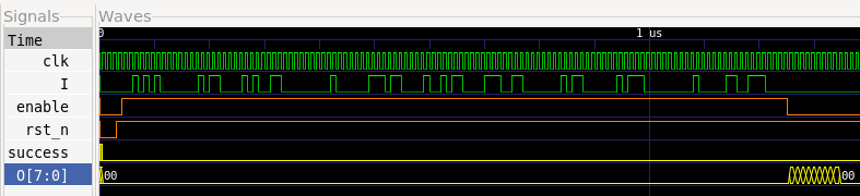
That is, the chip ingests 121 bits of serial input and then outputs a few bytes
of output. The serial output cleanly decodes as ASCII text and in the example
VCD it says TRY AGAIN. The success pin obviously stays unasserted.

Here it's pretty clear that our goal is to figure out what 121*A suspiciously square number bits as an input
make the success pin assert. There are two steps we need to take:
recover the netlist that can be simulated and then figure out which input sequence
makes the success pin assert.
Extracting the netlist#
To even be able to push input bits into the design, we first need to be able to simulate it. In theory, a GDS file is just a bunch of polygons-on-layers, denoting where the various semiconductor processes such as ion implantation or metal deposition happen. In this puzzle, this means 62131 polygons spread over 6 layers across a 190µm x 290µm area. At first glance, simulating this level of complexity seems to be a hopelessly difficult task. It sounds like it would require at least some ability to perform simulation of the underlying solid state physics or rather meticulous analysis of the geometries involved to figure out the circuitry.
Luckily, the synthesis process is significantly constrained: in practice, there are predefined "standard cells" that represent elementary logic operations such as "three input AND gate" or "D flip-flop". These cells are then placed on a uniform grid and wired together. These cells are available in a Process Design Kit which in this case is the SKY130 PDK (as is possible to either assume from the warmup part of the challenge or from the embedded metadata in the GDS file).
Opening up the GDS file in KLayout, we first observe an easter egg in the form of Morse code out of bounds of the chip spelling "PER ARENAM AD ASTRA". It's also convenient to install the SKY130A PDK plugin for KLayout, which preconfigures layer names, colors and connectivity and allows us to trace nets manually.

More importantly, we can observe that the GDS file contains a preserved list of cells with the original PDK names. This means that we do not even need to perform any sort of geometry matching at all, just look up the cell names in the PDK, read out where the connection pins end up and then trace the metal interconnects to figure out what is connected to what.
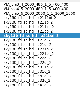
Now I got a bit suspicious here for a moment, but spot checking the geometry of the cell types in the GDS and in the PDK seemed to confirm that this corresponds to the actual SKY130 PDK available on the web.
At this point, I decided to commit and trust the labeling as-is and just extract the netlist from the GDS file.
This is a bit of tedious drudgery, but conceptually nothing complicated. We just need these pieces from the PDK:
- The layer assignments (which layers are metal interconnects and which contain the cells and how the vias are defined in between layers)
- Cell pin locations: those come from special "LEF" files in the PDK and basically say "this cell has a pin called A1 with this geometry on this layer". I had to merge the "magic" and the not-magic LEF files to get the full picture, though I expect the original GDS files were generated using a flow that comes with these cells pre-merged.
Then we proceed to:
- Parse the GDS file via gdstk and extract all the layers and polygons and the "cut layers". Those are essentially "vias", layers connecting two metal layers together. Also keep track of the cell names that match the PDK cell names, noting their locations.
- Figure out in-layer connectivity: which polygons intersect and thus belong to the same net. Shapely's STRtree helps here.
- Connect the layers together via the cut layers. For every shape on the cut layer, figure out which nets on the two metal layers it connects and merge those nets together.
- Next we return back to our list of PDK cells and their locations. Parsing the PDK's LEF files, we know where the individual pins of the cells are located in the design.
- For every pin, we check which net it is connected to, that is, which net polygon it intersects (on the appropriate layer only!). At this point, we can also do a sanity check that exactly one output pin drives each of the nets.
- Go through the text labels denoting the input (also present in the GDS) and use them to figure out which nets are the IO.
- Finally, this gets serialized to a Yosys compatible JSON netlist
All told: 738 sky130 logic cells connected together got extracted at this step.
Running the netlist#
To validate that the netlist is correct, we need to simulate it. Zeroth step
is converting the Yosys JSON netlist to Verilog. This is done simply
via yosys -p "read_json puzzle.json; write_verilog puzzle.v".
At this point, we have a Verilog file that has an interface like this:
module puzzle(
   input wire clk,
   input wire enable,
   input wire I,
   input wire rst_n,
   output wire [7:0] O,
   output wire success
);
Its content is just an endless list of 738 sky130 logic cells connected together:
// ..
sky130_fd_sc_hd__a21o_2 a21o_2_x166060_y89760 (
  .A1(net544),
  .A2(net545),
  .B1(net505),
  .X(net546)
);
sky130_fd_sc_hd__a21o_2 a21o_2_x167900_y255680 (
  .A1(net505),
  .A2(net527),
  .B1(net506),
  .X(net90)
);
// ..
This is obviously rather unhelpful. However, since we have the reference Verilog functional models for every cell type from the PDK and the netlist that wires them together, we are free to simulate the circuit and observe its behavior.
I first made a simple cocotb-based harness that instantiates the puzzle, feeds in an input and prints the decoded output:
@cocotb.test()
async def feed_bits(dut):
    cocotb.start_soon(Clock(dut.clk, CLK_PERIOD_NS, unit="ns").start())
    clkedge = FallingEdge(dut.clk)

    bits = get_input_bits()
    dut._log.info("feeding %d bits: %s", len(bits), "".join(map(str, bits)))

    # Reset and enable the DUT, just like in the example VCD
    dut.I.value = 0
    dut.enable.value = 0
    dut.rst_n.value = 0
    await clkedge
    for _ in range(3):
        await clkedge
    dut.rst_n.value = 1
    await clkedge
    dut.enable.value = 1

    # Feed in the input bits
    for b in bits:
        dut.I.value = b
        await clkedge
    dut.enable.value = 0
    dut.I.value = 0

    # Read the output bytes and print them out
    out = []
    for i in range(NBYTES):
        await clkedge
        byte = sample(dut.O)
        out.append(byte)
        dut._log.info("byte %2d: O=%s success=%s", i,
                      f"{byte:02x}" if byte is not None else "xx",
                      str(dut.success.value))

    text = "".join(chr(b) if b is not None and 32 <= b < 127 else "." for b in out)
    hexs = " ".join(f"{b:02x}" if b is not None else "xx" for b in out)
    dut._log.info("O bytes hex:   %s", hexs)
    dut._log.info("O bytes ascii: %s", text)
This confirmed that it is possible to execute the puzzle and observe the expected "TRY AGAIN" output.
...
7875.00ns INFO     cocotb.puzzle                      O bytes ascii: TRY AGAIN.......................
...
At this point, I found it sufficiently believable that the extracted netlist is the correct one. Onto the next step.
Enter SymbiYosys#
Manually figuring out what each subcomponent of the circuit does would surely be enlightening. But I had places to be, so I decided to invoke heavy machinery: formal verification tools. Abstractly, these tools allow the user to specify certain invariants about their circuits and then prove that they actually hold.
In our case, we are going to be asking a question of the form "is there any input sequence that makes the success pin assert?". Internally SymbiYosys does this by unrolling the circuit for a certain number of time steps ("depth") into a combinational circuit and then handing the formula to a SMT solver.
In practice, we get several special functions into our Verilog to use. For our use case,
cover is the one we want: it allows us to specify a statement that we
would like to be true at some point. So we can just specify cover(success).
To specify the input sequence, we can use a SymbiYosys special annotation
(* anyconst *) on a wire internal to our harness. This will tell
the tool that this wire can take on any value to achieve the stated goal.
In short, the wrapper harness looks like this:
module sby_wrapper(input clk);

(* anyconst *) wire [120:0] input_data;

reg [8:0] counter = 0;
reg rst_n;
reg enable;
reg I;

wire success;

puzzle p(
  .clk(clk),
  .rst_n(rst_n),
  .enable(enable),
  .success(success),
  .I(I)
);

always @(*) begin
  rst_n = 0;
  enable = 0;
  I = 0;
  if (counter < 3) begin
    rst_n = 0;
    enable = 0;
  end else if (counter < 4) begin
    rst_n = 1;
    enable = 0;
  end else if (counter < 4 + 121) begin
    rst_n = 1;
    enable = 1;
    I = input_data[counter - 4];
  end else begin
    rst_n = 1;
    enable = 0;
  end
  cover(success);
end

always @(posedge clk) begin
  counter <= counter + 1;
end

endmodule
Next, we need to configure SymbiYosys itself. This is done using a special .ini format configuration file.
We are interested in how many time steps do we want to check for. Since we have the reference VCD trace, we have a good idea of how many steps does it take for the circuit to process the input and do something.
[options]
mode cover
depth 200
append 50
We also need to convince SymbiYosys to read the PDK files specifying the cells and our extracted Verilog netlist.
[script]
read_liberty -ignore_miss_func -ignore_miss_dir pdk/sky130_fd_sc_hd/timing/sky130_fd_sc_hd__tt_025C_1v80.lib
read -formal sby_wrapper.v puzzle.v
prep -top sby_wrapper

[files]
sby_wrapper.v
puzzle.v
As for the engine, I picked one at random and it produced a solution in under two minutes. I have heard through the grapevine that selection here actually matters and some of the available engines can be too slow.
[engines]
smtbmc bitwuzla
This config file can then just be executed by running:
sby -f config.sby
This produces a solution that makes the success pin assert. I was definitely not expecting this to work, but it did.
SBY 23:46:22 [/tmp/tmp7836y_vb] engine_0: ##   0:01:42  Writing trace
to Verilog testbench: engine_0/trace0_tb.v
SBY 23:46:22 [/tmp/tmp7836y_vb] engine_0: ##   0:01:42  Writing trace
to constraints file: engine_0/trace0.smtc
SBY 23:46:22 [/tmp/tmp7836y_vb] engine_0: ##   0:01:42  Writing trace
to Yosys witness file: engine_0/trace0.yw
SBY 23:46:25 [/tmp/tmp7836y_vb] engine_0: ##   0:01:45  Status: passed
SBY 23:46:25 [/tmp/tmp7836y_vb] engine_0: finished (returncode=0)
SBY 23:46:25 [/tmp/tmp7836y_vb] engine_0: Status returned by engine: p
ass
SBY 23:46:25 [/tmp/tmp7836y_vb] summary: Elapsed clock time [H:MM:SS (
secs)]: 0:01:45 (105)
SBY 23:46:25 [/tmp/tmp7836y_vb] summary: Elapsed process time [H:MM:SS
 (secs)]: 0:01:57 (117)
SBY 23:46:25 [/tmp/tmp7836y_vb] summary: engine_0 (smtbmc bitwuzla) re
turned pass
SBY 23:46:25 [/tmp/tmp7836y_vb] summary: cover trace: /tmp/tmp7836y_vb
/engine_0/trace0.vcd
SBY 23:46:25 [/tmp/tmp7836y_vb] summary:   reached cover statement sby
_wrapper._witness_.check_cover_sby_wrapper_v_39_4534 at sby_wrapper.v:
39.5-39.19 step 126
SBY 23:46:25 [/tmp/tmp7836y_vb] Removing directory '/tmp/tmp7836y_vb'.
SBY 23:46:25 [/tmp/tmp7836y_vb] DONE (PASS, rc=0)
We get a VCD trace that shows that the success pin asserts and the output now yields "(* TWO STARS *)" instead of "TRY AGAIN".

To avoid having to extract the input bits from the VCD, we can also poke at the
Yosys witness file by running yosys-witness display trace0.yw which shows (MSB is the last bit fed in):
#0 input_data[120:0] = 0000000101000100100000100000010000000100001010000010000001000001000000101000000000000101010100000000000010000101010000000
What does this all mean?#
Doing the challenge like this is somewhat unilluminating: sure, I got the answer, but what does it mean? Googling around, I found this 2023 article about a logic game that asks the player to assign stars to a grid such that there are exactly two stars in each row and column without touching (with some more constraints given by regions drawn on the puzzle map).
Displaying the found 121 input bits as an 11x11 grid indeed reveals that the input is a solution to a puzzle of this type.
·······★·★·
★····★·····
·······★·★·
★·★········
····★·★····
··★·····★··
····★·····★
·★····★····
···★······★
·····★··★··
·★·★·······
First check: proving that this is a unique solution accepted by the chip. With this setup, sby yields a cover trace, not all of them. Slight modification of the Verilog harness
cover(success && input_data != <the found solution>);
allows us to check that this solution is unique, at least within the bounded 200 timesteps we have configured and under this input/success/reset timing. This means that the design enforces some additional constraints in addition to "two stars per row and column without touching" that point to this exact solution.
Second check: placing this unique solution on the 2023 puzzle grid does not yield a valid solution nor any meaningful message (even under any D₄ symmetry).
Everything else#
I decided to wrap the solver in a script and force it to enumerate the inputs.
This is implemented primitively by adding a successive
assume(input_data != <previously found solution>) to the Verilog harness and
rerunning sby until it fails to find any input that does not produce the default "TRY AGAIN" string.
This resulted in
- All zeroes yield "EMPTY SKY"
- All ones yield "BIG BANG"
- Some of the configurations that satisfy the "two stars per row and column" but not the "no adjacent stars" constraint yield "TWO NOT TOUCH". I expect that this is the case where the internal regions I do not know are satisfied, but the stars touch each other.
Inputs shorter than 121 bits seem to not produce any output, inputs longer than 121 bits seem to take into account only the 121-bit prefix.
Curiously, the VCD is dated at December 2016 (the leap second of the month actually). This points to a puzzle called Star Search on the Jane Street puzzle webpage. But not quite sure if there is any way to extract something further from this. The previous November 2016 puzzle does actually feature a 11x11 grid, but again, placing the stars of the solution on it does not yield any meaningful message.
Overall, I am not quite sure if extracting a region map or some other constraints that govern the uniquely accepted solution would produce any further insight. It's likely that this would now require actually reverse engineering the circuit subcomponents, but that is an entire rabbit hole I do not have time to go down at this point. Excited to see what other write ups uncover about the puzzle.