Hardcaml to 74-series logic
Update (Feb 2026): This project was selected as one of the winners of the Jane Street's Advent of FPGA Challenge!
This is a PCB solving the Day 1 Advent of Code 2025 puzzle using 125 discrete 74-series logic chips. This board was constructed by an automated flow going from Hardcaml source code to fabricated, assembled hardware.
This project implements an automated synthesis flow targeting logic slices constructed from discrete 74-series logic chips. The pipeline takes arbitrary Hardcaml source code and produces a PCB design ready for fabrication. The same physical board template can realize any design that fits within its 121-slice budget, with only the LUT resistor values and the inter-slice autorouted connections changing between designs.
The project is built for the Advent of FPGA, demonstrating the pipeline by solving the Day 1 puzzle of the 2025 Advent of Code.
The basic idea is simple: build what is effectively a sort of an old school Gate Array, using 74-series multiplexers as LUTs, configured by resistors, and 74-series D-flip flops to construct a regular grid of identical logic slices. Then, the interconnects between the slices are autorouted as needed for any specific design.*It is theoretically possible to synthesize directly to raw 74-series logic chips via 74xx-liberty, but this gets us a netlist only, with no placement or routing tools available.
The flow chains standard open-source tools, with Yosys for synthesis, nextpnr for placement and routing, finishing with KiCad and FreeRouting for PCB design and autorouting.
The problem and the solution#
The project requires a rather simple AoC puzzle. Even a "sort a list" puzzle would blow up the resource budget beyond reasonable limits. Historically, maybe one puzzle of the first few days of AoC has been a good fit. This year, Day 1 easily qualifies.
The problem is simple: we are given a combination lock with a single dial and a series of instructions telling us the direction and how many clicks to advance the dial by:
L68
L30
R48
L5
R60
...
The end result is counting how many times the dial ended up at zero after performing an instruction in the list.*Or, in the second stage, any time it hits zero during any of the steps. This is logically simpler but the output counter needs to be larger, eating up more slices, so I went with the first part.
The solution idea is simple: I wanted the logic to actually contain the dial state and to actually advance it by one every clock cycle. This way, we get cool looking blinking LEDs which provide observable intermediate state for every constituent slice.
For the interface, we go line-by-line, presenting the number of clicks and the direction to the input ports. Then, we assert a "valid" signal for a single clock cycle, loading it to the internal register. Then, we wait a constant amount of clock cycles and then load the next line. The solution deliberately omits flow control, to make the interface unidirectional and to minimize resource usage.
I sized the registers to fit my specific input, 10 bits for the input and 11 bits for the output counter. The challenge itself does not mandate any specific ranges.
Although originally, I wrote the design in Verilog, I rewrote it in what is probably the least canonical Hardcaml ever after I realized the timelines are going well. I had to use the preview version of Hardcaml (0.18), as the current release does not support initial values for registers. Without this, either some expensive reset logic would need to be synthesized, blowing up the design resource usage, or alternatively reset inferrence would need to be added to nextpnr-generic, which is too complicated given the time constraints.
One limitation surfaced: Hardcaml's Verilog output lacks Yosys-compatible "src" attributes, so slice-to-source-line annotation is not possible. The resource usage overhead was negligible, only a few more slices than the old Verilog solution.
Getting nextpnr to work#
Now that we have the HDL sorted, the complex part may begin: configuring nextpnr to handle our custom architecture. Luckily there is some very good news: in addition to all the various real FPGA architectures, nextpnr also has a generic architecture. The deal is simple: we get a Python API that allows us to specify the slice placement and the interconnects between them. We do not really get to choose the slice architecture: they are fixed to be a fairly standard LUT-into-DFF combo.
More concrete slice design#
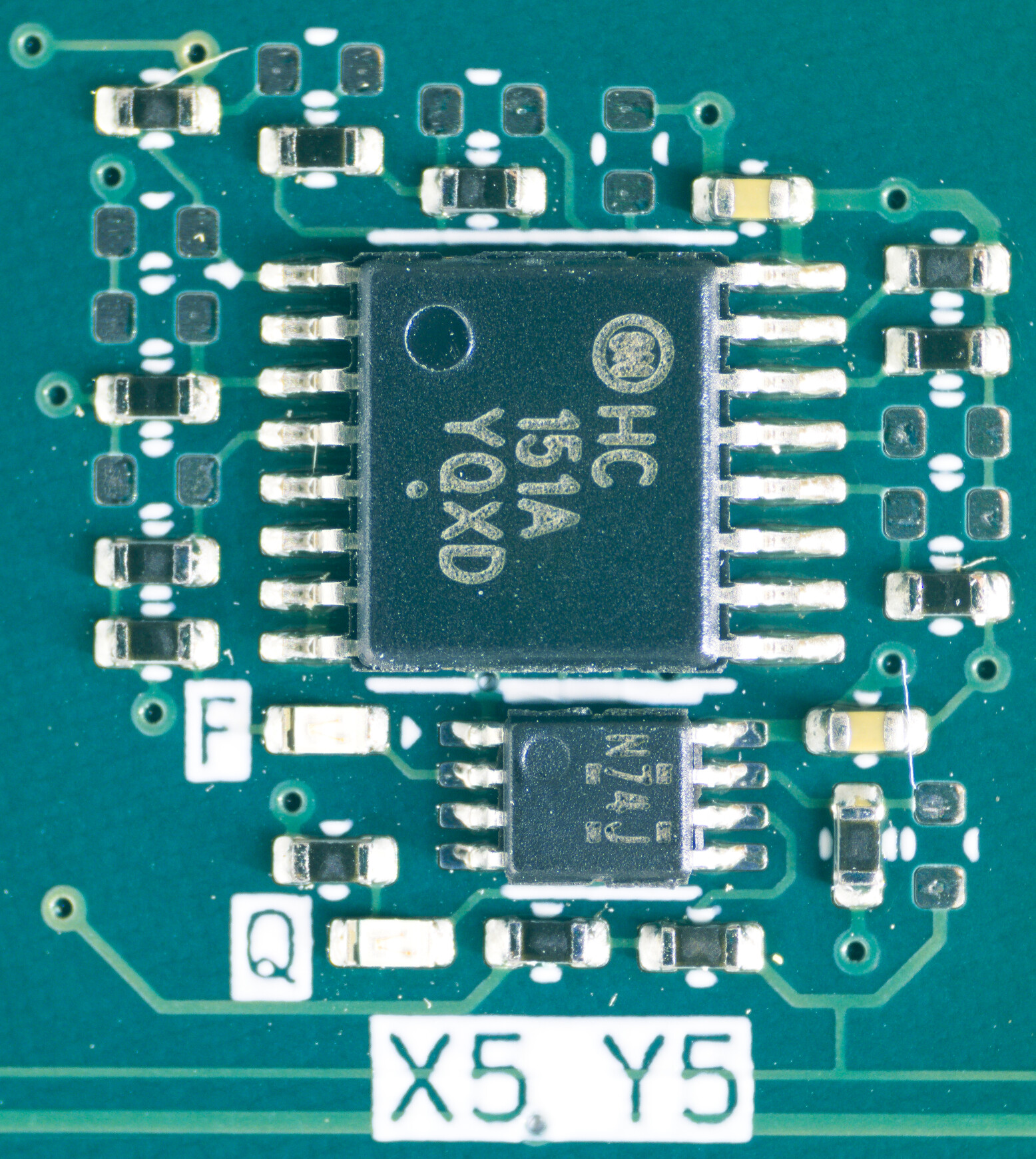
It is at this point where I figured it is important to nail down the actual slice components. Although sharing a DFF between multiple LUTs would reduce the total component count, using a single DFF per LUT simplifies the slice design considerably. I decided to go with the SN74LVC1G74, a single DFF in a tiny VSSOP-8 package, available for $0.13 at JLCPCB with tens of thousands in stock.
Next, the LUT design. In practice, there are two reasonable ways to go about this:
- Use a decoder and a diode matrix to implement the truth table. This is "the classic" way to do ROMs, but as it turns out 74-series decoders are not that common these days. And we are effectively paying "per chip" anyway.
- Use a multiplexer as the LUT. The inputs are connected to Vcc or GND through resistors to set the truth table. The good news is that multiplexers are plentiful, and available in modern high density packages. For example the MC74HC151ADTR2G can be had for $0.19 and there are thousands in stock at JLCPCB.
There is a degree of freedom here: picking the amount of inputs to the LUT. The default nextpnr-generic example uses 4-input LUTs, but as it turns out muxes that can implement 4-input LUTs (16-to-1 muxes) are somewhat unusual, meaning it is much more practical to go with 3-input LUTs.
Describing the architecture to nextpnr#
The next step is to describe the architecture to nextpnr. This is essentially done by writing a Python script that adds the various elements to the architecture. The API for nextpnr looks like this:
# Create wires for the slice's ports
ctx.addWire(name=f"X{x}Y{y}_F", type="BEL_F", x=x, y=y)   # LUT output
ctx.addWire(name=f"X{x}Y{y}_I0", type="BEL_I", x=x, y=y)  # LUT input

# Create the slice (LUT + DFF combo)
ctx.addBel(name=f"X{x}Y{y}_SLICE", type="GENERIC_SLICE",
           loc=Loc(x, y, 0), gb=False, hidden=False)

# Wire the ports
ctx.addBelOutput(bel=f"X{x}Y{y}_SLICE", name="F",
                 wire=f"X{x}Y{y}_F")
ctx.addBelInput(bel=f"X{x}Y{y}_SLICE", name="I[0]",
                wire=f"X{x}Y{y}_I0")
A few words should be said about the interconnects. In standard FPGA architectures, there are fixed amount of "wires" going inside of the fabric, with the individual slices being connected to them through programmable switches. In my case, I am adding the wires on an "as-needed" basis with an autorouter on the resulting PCB.
In practice, I implemented this by each slice having a bunch of "local" wires that allow it to interconnect with its neighbors and then having a set of "global" wires that can connect to any slice. Hopefully the "local" wires are going to steer nextpnr to mostly place logically connected slices physically close to each other.
Of course those wires do not physically exist when nextpnr is deciding the placement, but realistically, given the dimensions of the PCB being what it is, I expect that almost any reasonable routing can be achieved.
Note that I do not care about timing nor fanout restrictions. In practice, I am just going to run the design as slow as needed, allowing signals to settle for however long it takes.
After some tuning of the locality constraints, I got nextpnr to synthesize the design correctly. The end result uses about 100 slices, which is about what I expected (I wanted the board to be something like 10x10 slices). There is also a bit over 100 nets, which is reasonably easily routable on a 4-layer PCB of this size. The allocation looks like this:
Where the black dots are slices with DFF enabled. What stands out is the triangle in the bottom right: this is the output counter. Presumably since there is very little coupling between the output counter and the rest of the design, nextpnr figured it is advantageous to cluster it right next to the output bits.
In total, this works out to 96 slices, out of which 29 have DFFs enabled. This exactly corresponds to the 7 bits of the dial state, 11 bits of the output counter, 10 bits of the step count register and 1 bit for the step count sign in the source code.
On inputs and outputs#
What remains is convincing nextpnr to properly handle the inputs and outputs of the design. The generic architecture is assuming that there are bidirectional "IO" slices and just allocates those to the top level module inputs and outputs. But, for ease of use, I want to have them allocated statically and to have outputs and inputs on different sides of the PCB. This is done by placing special attributes on the top level module ports, for example:
(* BEL="X0Y6Z0_IO" *)
input wire step_count_9
Designing the "blank slate" PCB#
Now that I have confirmed that it is possible to synthesize and place and "route" the design, there was no time to waste. The next step is to design a "blank slate" PCB. This is a grid of slices with power routing and clock and reset lines, ready to be customized for any specific design by changing the LUT resistor values and autorouting the inter-slice connections.
Due to how regular the design is, this is mostly about routing an individual slice and then using the replicate layout plugin to make 121 copies of them (an 11x11 grid of available slices).
The idea is to have a 4-layer PCB, with the stackup being:
- Top: components + clk + rst + IO blinkenlights
- Inner 1: Vcc + GND
- Inner 2: autorouted signals
- Bottom: autorouted signals
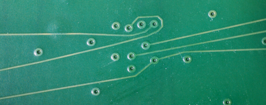
This way, I can cleanly separate the "template" from the autorouter work by layer. The slices are just tightly packed clusters of resistors around the multiplexer and the DFF. The inputs and outputs are dropped by a via to the bottom two layers, ready for the autorouter to connect them. This is how a single slice looks like in real life (crossover with a different project):
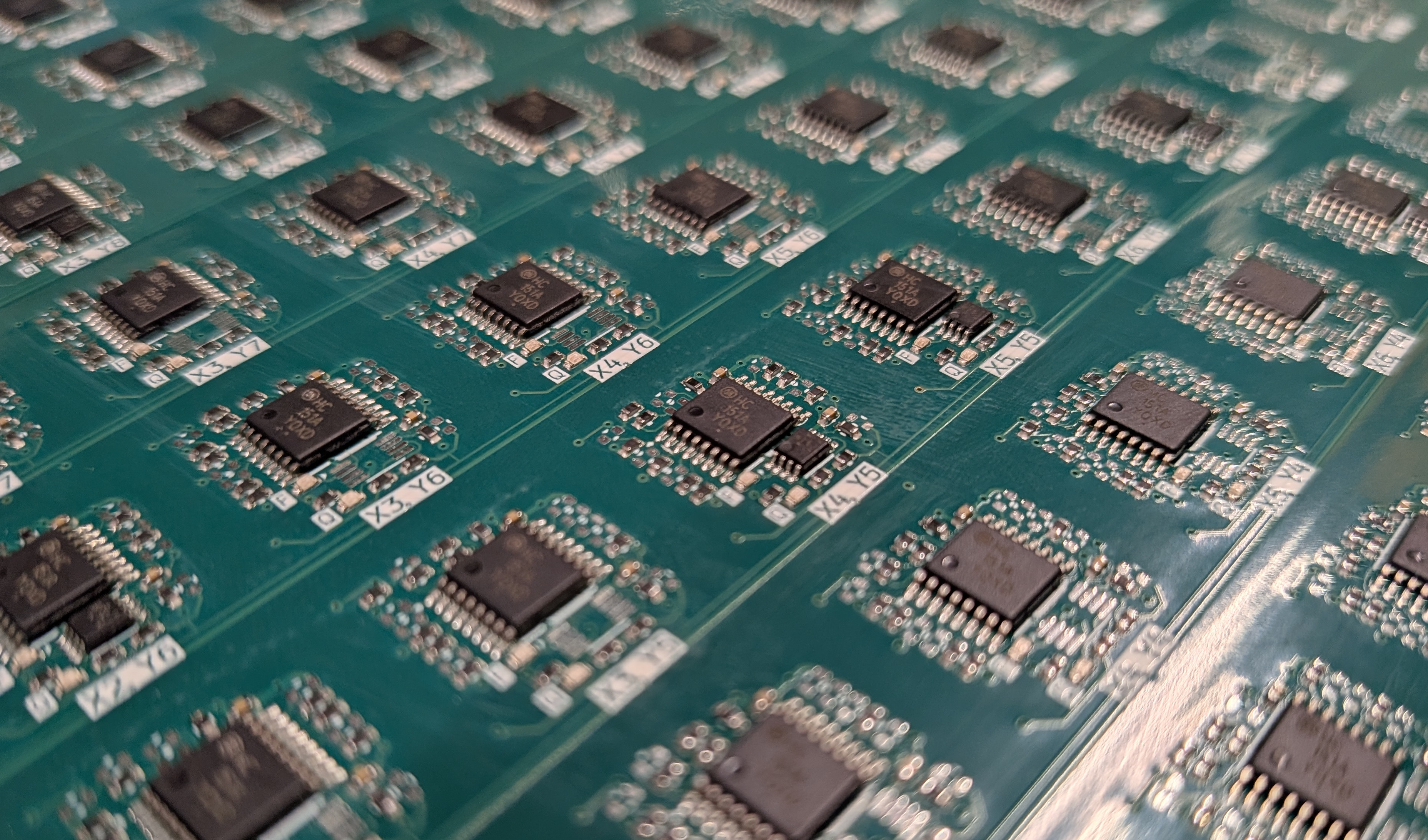
The entire sizeable 20x17cm PCB template then ended up like this:
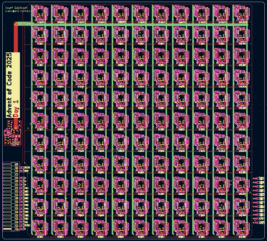
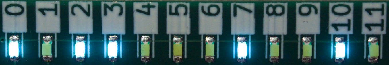
The IO interface is spartan, with a single header for the inputs and LEDs displaying the result in binary. This way it can be easily interfaced to a microcontroller or a single board computer.
Translating nextpnr output to KiCad#
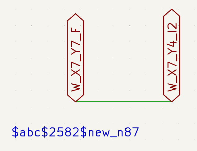
For the net lists, what we are looking at here are nets that look approximately like this:
"$abc$2582$new_n87": {
  "hide_name": 1,
  "bits": [ 71 ] ,
  "attributes": {
     "ROUTING": "X7Y7_F;;1;LOCAL_X7Y4_X7Y7_1;LOCAL_X7Y4_X7Y7_1_FROM_X7Y7_F;1;X7Y4_I2;LOCAL_X7Y4_X7Y7_1_TO_X7Y4_I1;1"
  }
}
This effectively says that we have to connect the "F" output of the "X7Y7" slice to the "I2" input of the "X7Y4" slice. The rest is no longer relevant --- those were just imaginary wires I used to steer nextpnr to get at least a semblance of reasonably local placement.
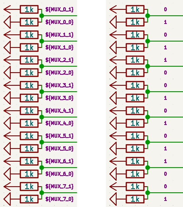
The most straightforward way I figured is to add global labels to the KiCad schematic for each of the slice ports, like this:
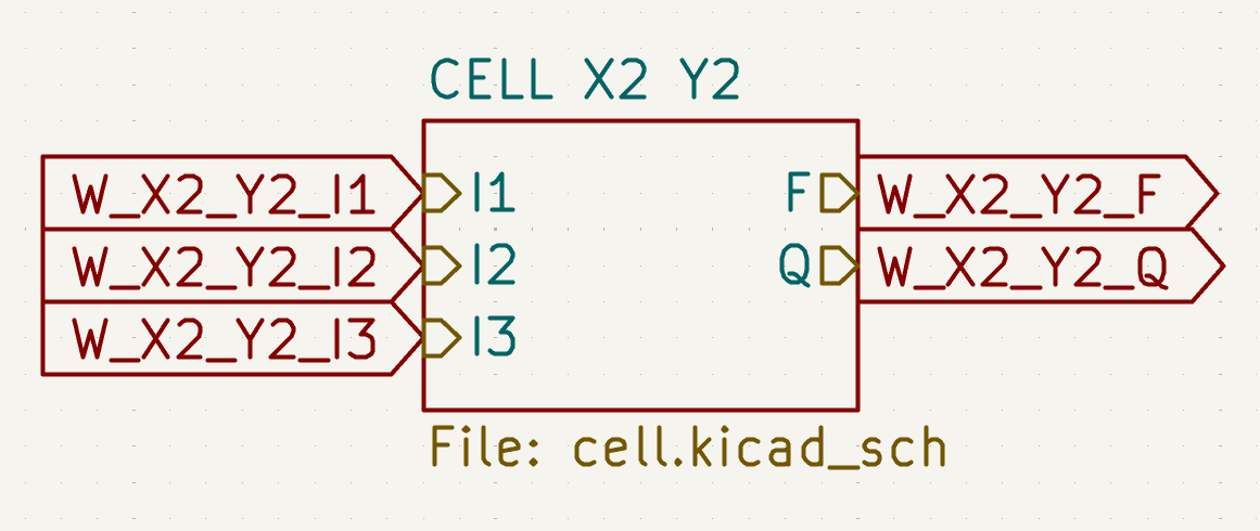
Then, a script using the kiutils library goes through the nets in the nextpnr output JSON and creates a special schematic file that simply wires up the global labels according to the nets, by creating a long linear wire with the labels hanging off of it, like so:
The next step is actually configuring the LUTs. This is done by adding schematic fields for each bit to the slice schematic instances. Then, those are transferred to the individual resistors field I call "POPULATE". Then, I just exclude or include resistors from the BoM depending on the POPULATE field value. In theory, just wiring the resistors to Vcc or GND and letting a strategically placed zone do the rest would work with less space, but resistors make post-manufacturing surgery easier and allow per-slice reconfiguration.
In addition to the netlist wiring and the LUT configuration, I decided not to populate the muxes and DFFs that are not required in this particular design. This makes the boards significantly cheaper to manufacture.
Running the FreeRouting autorouter#
The final step is routing the synthesized nets on the PCB. This means routing about a hundred nets on the two layers dedicated to signals that the template PCB has. FreeRouting handled this in about an hour of compute time, with some gentle convincing.
Evaluation#
The boards were manufactured and assembled by JLCPCB, arriving about two weeks after ordering, ready to be powered up and tested.
In short, the board worked as designed out of the box, computing the correct solution when given my AoC input. There is no heroic tale of debugging or patching with magnet wire, it worked as expected. This was my only chance, as the holiday timeline left no time for a second iteration.

I run it interfaced to a Raspberry Pi, with an OCaml script for bit banging the interface over the GPIO pins. The board consumes around 100mA, mostly independent of the clock speed, so it can be powered directly from the 5V header pin on the Raspberry Pi.
The board can be clocked up to around 100kHz before it starts to miscount. Running at that speed, it computes the result in around a minute and a half.
In theory, the DFFs have negligible setup and hold times of around 2ns. The MUXes should have propagation delays of around 50-250ns (highly Vcc dependent). The longest combinational chain in the design is around 10 slices long, which suggests that the maximum clock speed could be about an order of magnitude higher.
Probing and observing some of the internal signals with a higher clock speed shows that the settling time of the combinational chains can be in the low hundreds of nanoseconds, as expected and illustrated below:
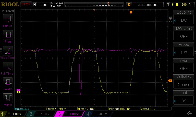
In the end, the observed 100kHz limit appears to be mostly due to timing jitter induced by the bit banging process on the Raspberry Pi side. With a more stable controller, or some PREEMPT_RT magic on a properly configured Linux kernel, one could likely push the speed significantly higher.